Introduction
The transport theory of semiconductors based on the band theory of solids which was first formulated in 1931 by Wilson, was later applied to the metal/semiconductor contacts. In 1938 Schottky suggested that the potential barrier could arise from stable space charges in the semiconductor without the presence of a chemical layer. The model arising from this consideration is known as the Schottky barrier. At the same time Mott devised an appropriate theoretical model for swept-out metal/semiconductor contacts that is known as the Mott barrier.
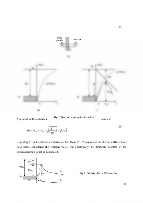
Because of their importance in direct current and microwave applications and as tools in the analysis of some fundamental physical parameters, metal/semiconductor contacts have been extensively studied.
1. Metal/Semiconductor Contacts (M/S)
The M/S contact is an important part of the electronic and optoelectronic devices, either as an active element or as a charge carrier collector. The M/S interface processes and the diffusion potential value at the M/S contact depend on two factors:
a) The difference between the metal work function M and the semiconductor work function S;
b) The presence of the surface states in the semiconductor
These two factors act simultaneously, but for simplicity limiting cases involving one factor or the other are analysed.
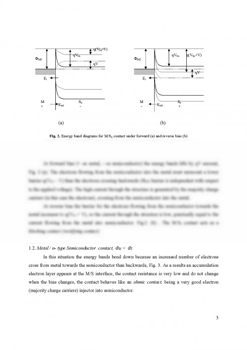
1.1. Metal / n- type Semiconductor contact, M > S.
The energy band diagram before and after contact is shown in figure 1, where ICn is the semiconductor ionization energy; M is the metal work function; Sn is the semiconductor work function; Sn is the electron affinity of the semiconductor (measured from the bottom of the conduction band to the vacuum level); Eg is the energy gap and n is the semiconductor chemical potential.
The semiconductor work function being lower than the metal work function, the electrons flow from the semiconductor towards the metal generating a negative charge inside the metal and a positive one in the semiconductor. As a result, an electric field appears at the interface M/S, oriented from semiconductor towards metal. At equilibrium this field opposes to the diffusion of the electrons into the metal. At the M/S interface, the energy bands bend up due to the depletion of electrons in the semiconductor. The electrons flowing towards the metal must cross over a barrier height bn. This “built-in barrier” related to the barrier potential is:
(1)
On the other side the barrier height for the electrons flowing from the metal into the semiconductor is:
(2)
The metal-semiconductor electron barrier is higher than the semiconductor-metal one. Because the charge carrier concentration in semiconductor is lower than the carrier concentration in metal, the depletion layer w0 extends only inside of the semiconductor.
Materialul este in limba engleza si a fost prezentat la o intrunire in Japonia legata de "bazele nanotehnologiei". Materialul nu are un caracter introductiv, ci prezinta in mare generalitati, dar la un nivel putin peste intermediar.
Documentul este oferit gratuit,
trebuie doar să te autentifici in contul tău.